TERASUN technology
ADVANCED LIGHT MANAGEMENT
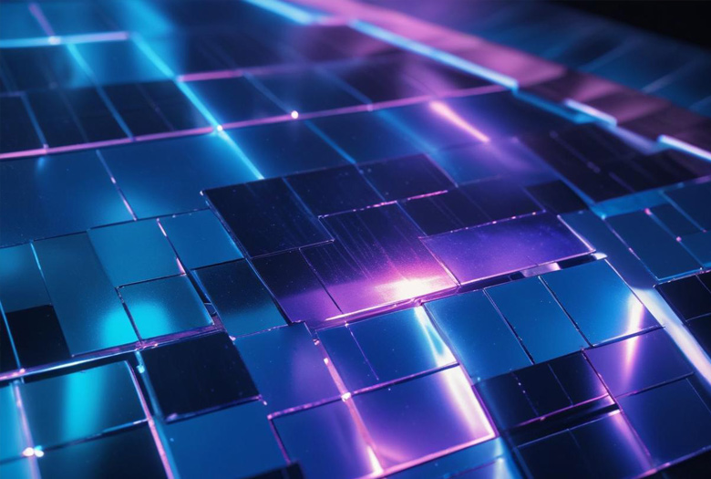
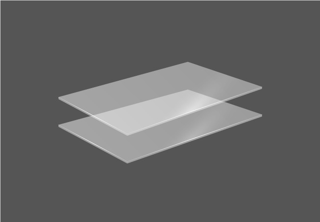
To maximize light absorption and improve efficiency in c-Si wafers and PV modules, TERASUN will develop advanced light-trapping techniques.
This involves developing micro- and nano-structuring methods using low-cost wet chemical etching or plasma-based processes for crystalline silicon wafers. These will significantly help improve the light-trapping inside the cells, thereby enhancing the photocurrent while maintaining high cell voltages. Additionally, the project aims to reduce cell-to-module losses by applying nano-photonic structures to the cover glass, thereby improving its durability and reducing maintenance costs.
PASSIVATING CONTACTS AND DIRECT BANDGAP ARCHITECTURES
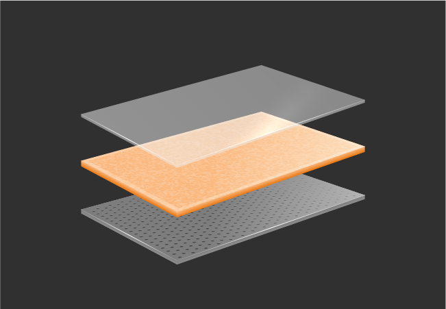
TERASUN will develop novel passivating contacts for efficient carrier extraction and recombination suppression, thereby maximizing photovoltage and efficiency.
The project will explore advanced materials, including nanocrystalline silicon and metal oxides, for their favourable properties such as wide work function range and good electronic properties. The development will focus on creating high-efficiency, low-cost IBC SHJ devices, optimizing surface passivation, and integrating indium-free transparent conductive oxides.
COPPER METALLIZATION FOR TERAWATT PRODUCTION SCALE
To address the limitations of silver in large-scale PV production, TERASUN will develop a copper electro-plating process.
This approach aims to reduce costs and improve performance with ultra-fine metallic contacts, compatible with temperature-sensitive SHJ solar cells. The project will focus on achieving high throughput and sustainability, including reducing material usage and environmental impact.
INDIUM-FREE TRANSPARENT ELECTRODES
The project will investigate both sputtering and slot-die coating processes for indium-free transparent conductive oxides.
These methods aim to provide highly conductive and transparent layers essential for SHJ solar cells. TERASUN will develop post-processing techniques, such as thermal treatment and laser-based crystallization, to optimize these TCO layers for high efficiency and industrial scalability.
TERASUN
TERASUN's technological advancements include:
- Advanced light management for c-Si and cover glass surface structures,
- Metal-oxide-based tunnel junctions and passivation for advanced c-Si textures,
- High-throughput, double-sided Cu-plating, and
- In-free TCO layers by sputtering or slot-die coating.
These developments will elevate the technology readiness level (TRL) of several crucial PV-related technologies, making significant strides towards sustainable and efficient solar energy solutions.